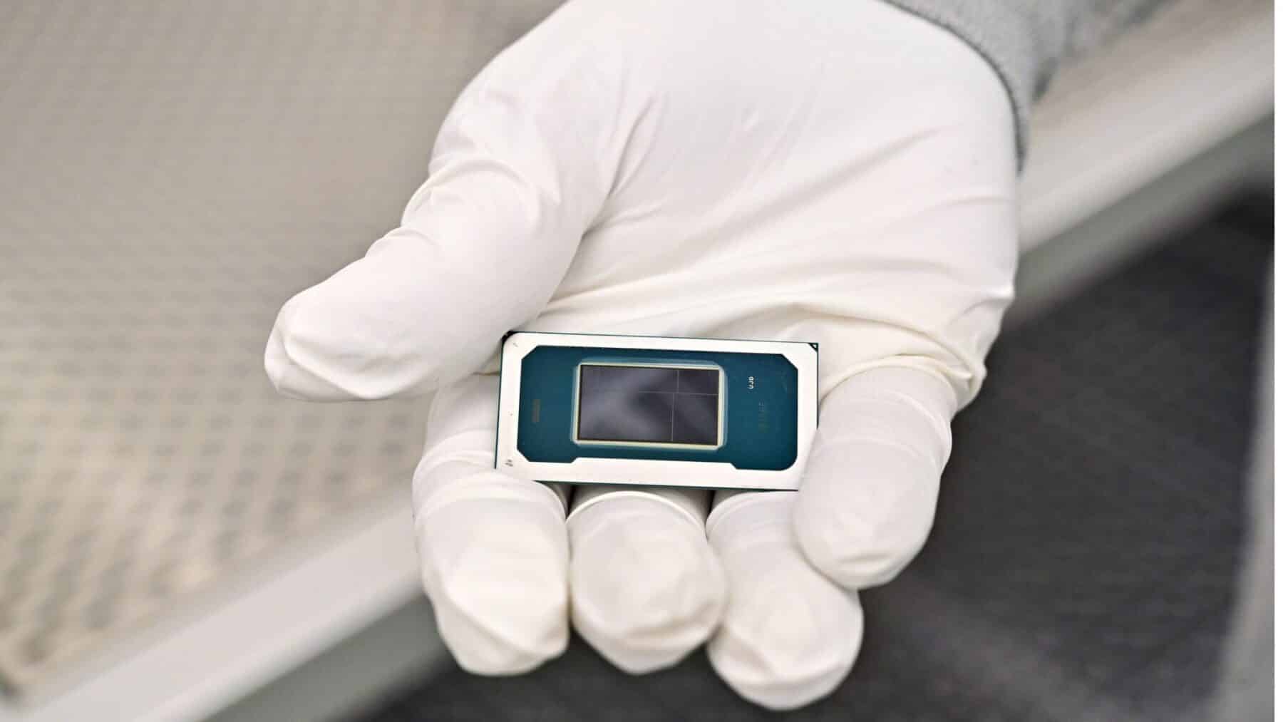
Flip a laptop over and nothing about the hinge or the keyboard hints at what just changed underneath the lid.
Inside the processor, the wiring itself has been turned around.
Power no longer travels the same path as the signals telling the chip what to compute.
Instead it arrives from the opposite side of the silicon entirely.
That rerouting just shipped inside millions of new laptops.
So how does flipping the wiring actually make a chip faster?
How moving the wiring to the back of the chip actually works
For decades, every wire on a processor, the ones carrying electrical current and the ones carrying data, shared the same side of the silicon. As transistors shrank, those two jobs started fighting for the same real estate, and cramped signal paths began losing ground to the fatter wires that power needs to avoid overheating.
The fix is almost mechanically simple once you see it: flip the chip’s power network to the underside of the wafer and leave the top entirely for signals. The chip designer’s version works by thinning the silicon wafer from below, then drilling microscopic vertical channels, called nano through silicon vias, straight up to each transistor.
That separation means engineers no longer ration space between the two networks. Power lines on the back can be built wider and more direct, cutting the resistance that bleeds energy away as heat.
The payoff shows up as cleaner, steadier voltage. An internal test chip built to prove out the approach achieved standard cell utilization of more than 90 percent over large areas of the die, packing far more usable transistors into the same chip area than a front-side design allows.
Where this is already sitting in your bag or on your desk
This is not a lab curiosity still years from a store shelf. The chip designer’s newest laptop chips, built on its latest manufacturing process, began shipping inside laptops this past January, with dozens of computer makers building them into new models.
So the backside power network proven out on that test chip is now part of the design running in machines people are typing on right now, not a future roadmap slide.
The company’s chief executive called the launch proof that Intel had delivered on its pledge to ship its first chips built on this manufacturing process on schedule. And the gain is not abstract. The company says the approach delivers 15 percent better performance per watt compared with the prior generation, a jump that shows up as either longer battery life at the same speed or more speed from the same battery.
Multithreaded tasks benefit even more, with more than 50 percent better multithreaded performance compared to the two previous laptop chip families, while drawing roughly 10 percent less power.
What the early test data actually showed before this went into real laptops
Before any of this reached a retail shelf, the company spent roughly two years validating the idea on a test chip built on an older, simpler manufacturing node. It was essentially a dry run meant to find problems before committing its flagship process to the design.
That early testing measured a 6 percent boost in clock frequency and roughly a 30 percent reduction in what engineers call voltage droop, the momentary power sag that happens when a chip suddenly demands a burst of current.
Those numbers matter. Voltage droop is exactly the kind of flaw a laptop owner never sees directly but feels anyway, as stutters or thermal throttling. Fixing it at the wiring level removes a problem no amount of software tuning can patch.
Rival chipmakers are chasing the identical idea under different names, confirming this is a shared industry pivot, not a one-company trick. One major foundry calls its version Super Power Rail, and another has its own backside design reserved for a future node.
Where the idea still hits real limits
None of this is free, and the limits are physical, not marketing spin. Thinning a wafer down to attach power from behind introduces new handling risks during manufacturing.
Engineers have had to invent fresh methods just to debug chips once the power grid is hidden on the far side of the silicon. Yield, the percentage of chips on a wafer that come out working correctly, was the biggest open question going in.
The company has said its early backside power test chips reached acceptable yield and debug times relatively quickly, a gap that closed faster than engineers initially expected.
Even so, this generation of backside power is arriving mostly in everyday laptop chips, not yet in the largest AI accelerators crunching through data centers, which still mostly rely on older wiring layouts. That split is itself worth watching, a shift GCN has covered recently this year.
What it means for the next chip in your pocket
The broader story here is less about one company’s bragging rights and more about a shared realization: chips had simply run out of room to keep doing things the old way.
Moving power to the back of the silicon freed up space nobody realized was being wasted. That has ripple effects beyond laptops, from the tiny processors inside smart glasses, a category GCN recently covered here, to the much larger AI server chips still waiting their turn.
What began as an obscure wiring decision is now something millions of people are carrying around without knowing it. The next refresh cycle will keep building on the same backside foundation, quietly making batteries last longer, one flipped wire at a time.
