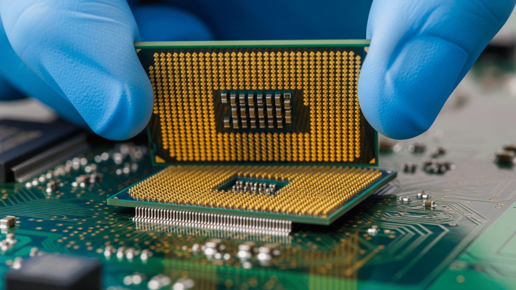
Every few years a chip arrives that works completely differently from anything that came before it, and most people buying the laptop that contains it never know.
That moment has arrived again.
A new processor has moved from the factory floor to store shelves, and the engineering change inside it is unlike anything in a consumer device before.
The numbers on the box look familiar. The mechanism underneath is not.
The chip that seemed like a normal upgrade
When a new laptop processor launches, the headline is usually a faster clock speed or a longer battery life.
Intel’s latest client chip, Panther Lake, looks that way at first glance.
Intel revealed the architectural details for its next-generation client processor, the Core Ultra Series 3 codenamed Panther Lake, and it is the company’s first product built on Intel 18A, described as the most advanced semiconductor process ever developed and manufactured in the United States.
That phrase “most advanced” gets used a lot. This time the engineering behind it is genuinely different in kind, not just degree.
Intel 18A delivers up to 18% higher performance at iso power, 38% lower power at iso performance, and a 30% chip density improvement versus Intel 3.
Why shrinking the transistor alone stopped being enough
For decades, chipmakers squeezed more performance out of silicon by making transistors smaller.
That worked until the wiring connecting those transistors became the problem.
For decades, power and signal lines within a chip’s architecture have competed for the same resources, and by separating the two, chips can increase performance and energy efficiency.
Think of it as a city that put its water pipes and fiber-optic cables in the same trench. As the city grows denser, both systems suffer.
The use of backside power delivery enables more efficient vertical routing by offloading power lines from the front side of chips, freeing up space for signal routing and further compacting the layout.
Something had to give. Engineers at Intel had been working on a fix for years, and Panther Lake is the first consumer chip to carry it.
Two breakthroughs arrived at the same time
Intel 18A pairs two distinct innovations, and understanding either one separately misses the point.
18A combines RibbonFET gate-all-around transistors with PowerVia, Intel’s unique industry-first implementation of backside power delivery.
The transistor change, RibbonFET, is a new geometry where the gate material wraps entirely around the current channel on all four sides instead of three.
RibbonFET improves electrostatic control and drive scalability, enabling higher performance per watt, lower minimum operating voltage, and more efficient scaling across operating conditions, critical for battery-powered devices where every milliwatt counts.
But the second innovation, PowerVia, is the one nobody outside chipmaking circles has heard of, and it is arguably the bigger structural change in a generation.
The wiring has been moved to the back of the chip
Here is the reveal: Panther Lake’s power grid does not sit on the same side of the silicon as the data signals. It sits underneath, on the back of the wafer entirely.
The backside power rail separates power and signal wiring by shifting power lines to the back of the wafer. This tackles problems such as increased via resistances in the back-end-of-line, ultimately improving transistor performance and lowering power consumption, while also eliminating interference between data and power wires and increasing logic transistor density.
Intel 18A combines RibbonFET gate-all-around transistors with PowerVia, Intel’s unique industry-first implementation of backside power delivery. The Intel Foundry newsroom explains both technologies in a public primer published alongside the product launch.
The roughly 6% frequency gain from backside power delivery is about half what is typically delivered when a chipmaker scales down transistors from one technology node to the next, and PowerVia delivers it with no change to the transistors themselves.
The 18A process introduces Intel’s RibbonFET gate-all-around transistors and the industry’s first mass-production-ready backside power delivery network.
The chip is being made at Fab 52 in Chandler, Arizona, which is fully operational and set to reach high-volume production using Intel 18A, strengthening U.S. technology and manufacturing leadership.
For context on how far the leading edge has moved, AMD’s EPYC Venice reached a similar 2nm class on TSMC’s process, and NVIDIA’s Vera Rubin chips are already heading to cloud providers, so the race at this layer of the stack is intensely competitive.
What this means for the laptop sitting on your desk
The engineering story matters because the real-world result shows up in battery life and sustained speed under load, two things laptop buyers actually feel.
Refined gate, source/drain, and contact structures improve overall cell uniformity and integration density, and these enhancements collectively enable Intel 18A to deliver better performance-per-area and energy efficiency, supporting more advanced and compact chip designs.
Intel is already moving to an upgraded version of the same node: Intel 18A-P has entered risk production, meeting the timeline first shared with customers and partners. Intel 18A-P offers up to 9% better performance-per-watt compared to Intel 18A.
Intel CEO Lip-Bu Tan has said he expects commitments from multiple foundry customers in the second half of 2026, and shares rose sharply on reports that Intel reached a preliminary deal to make chips for Apple, which would mark a significant milestone for Intel’s foundry ambitions.
The chip in the next thin laptop you pick up may look identical to its predecessor on the outside. Flip the wafer over in your mind, and everything has moved.
