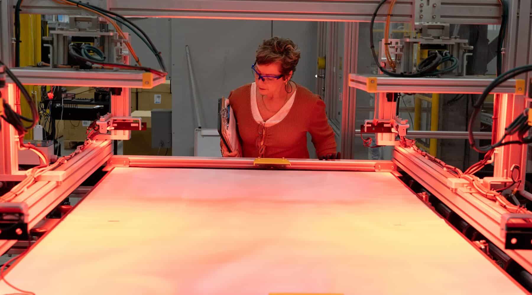
A block of gray silicon sits clamped above a grid of hair thin wires moving faster than a car on the highway.
Within minutes it will be sliced into hundreds of wafers thinner than a sheet of paper.
Most of what gets cut away never becomes part of a solar panel.
It becomes dust, swept into a slurry tank and often thrown out.
Factories across the country are now racing to build more of this capacity from scratch.
So what actually vanishes in that cut, and why does it happen on every single pass?
How a single saw blade erases more than a third of a block of silicon
Every solar wafer starts life as a cylindrical or squared off block of pure silicon, grown slowly from molten material into a solid ingot. To turn that block into usable wafers, manufacturers run it through a diamond wire saw, a tool that drags a single strand of wire coated in microscopic diamond grit back and forth across the block thousands of times, with the wire webs often moving at 15 meters per second.
That wire is not a knife. It is closer to a grinding tool, and every pass it makes carves out a channel of crushed, pulverized silicon that is too fine to ever be reassembled into a wafer.
Industry researchers call that channel the kerf, and it physically has to be wider than the wafer the saw is trying to produce. So even as factories have pushed standard wafers down to roughly 140 to 180 microns thick, the wire itself still eats away a comparable slice of material with every single cut.
Peer-reviewed research on diamond wire sawing puts that loss at roughly 35 to 40 percent of the silicon ingot, with some patent filings citing figures as high as 40 to 50 percent, disappearing before a wafer is ever lifted out of the machine.
Picture the factory floor where that lost silicon actually goes
Walk the length of an ingot sawing line and the loss is not abstract, it is a gray paste. Coolant and cutting fluid wash across the wire constantly, catching the shaved silicon and carrying it away as a thick slurry that pools in collection tanks beneath the saw.
That slurry is not clean scrap. It is a mix of crushed silicon, the silicon carbide abrasive once used in older slurry saws, steel fragments worn off the wire itself, and the fluid that carried it all away. Separating anything reusable out of that mixture is its own expensive chemical process, which is why most of it still gets thrown away rather than recovered.
Even the cleanest modern diamond wire lines, which replaced messier slurry based sawing years ago, cannot avoid the basic geometry. The width of the wire plus the grit bonded to it has to pass completely through the block, and that path can never return to being a wafer. It can only become waste or, with enough processing, a lower value byproduct.
Why this bottleneck matters more in US factories right now
This is not just an efficiency footnote, it is central to why America still struggles to build complete solar panels from scratch. The country’s module assembly lines can now put together far more finished panels than the country installs each year, but the ingot and wafer stage behind them has lagged badly.
Recent industry data puts domestic module manufacturing capacity at more than 75 gigawatts a year, while domestic cell capacity has only recently begun closing the gap, with newer industry tallies putting operational cell capacity at roughly 10.6 gigawatts and billions more under construction. Wafer slicing, the exact step where kerf loss happens, remains one of the thinnest links in that chain, with new domestic ingot and wafer plants only beginning to ramp output.
That gap is also expensive. Wafer slicing has historically eaten up a disproportionate share of the cost of getting from raw silicon to finished cell, since every ingot pays for wire, abrasive, and machine time regardless of how much usable wafer survives the cut. A polysilicon price floor set earlier this year only raises the stakes on every gram that turns into dust instead of product.
Where the mechanism runs into real limits
None of this means kerf loss is some industry secret nobody has tried to fix. Wafer thickness has fallen for two decades precisely because thinner wafers use less silicon per watt of eventual panel output, and diamond wire sawing itself replaced older slurry based cutting because it wastes noticeably less material and runs faster.
But there is a hard physical floor built into the process. Cut a wafer too thin and it becomes so fragile that it shatters inside the very machine meant to produce it, which is why commercial lines still hover in the 140 to 180 micron range rather than chasing the thinnest experimental wafers researchers have managed in a lab. Breakage during slicing adds its own hidden cost on top of the kerf itself.
Recovering silicon from the slurry is technically possible too, and has been studied for well over a decade. Yet separating usable silicon from the abrasive and metal contamination mixed into that paste has stayed expensive enough that most factories still do not bother, leaving kerf loss as a cost built into the price of every wafer rather than solved outright.
What it means for the next wave of US solar plants
None of this is likely to change overnight, and that is the honest takeaway. As more ingot and wafer plants break ground domestically, each one inherits the same physical limit that every silicon wafer factory on earth has lived with for years.
Even so, the economics are shifting in a way that makes the loss harder to ignore. As federal incentives push companies to build out the missing middle of the supply chain, the cost of every discarded gram of silicon becomes more visible inside a domestic factory’s books.
That visibility is sharper than it ever was when wafers were simply imported already finished. It is also why plants described in recent panel launches and new cell lines are being watched closely for how much silicon they actually waste, not just how many watts they eventually ship.
The saw blade has not gotten any gentler. What has changed is how closely American manufacturers now have to watch what falls away beneath it.
