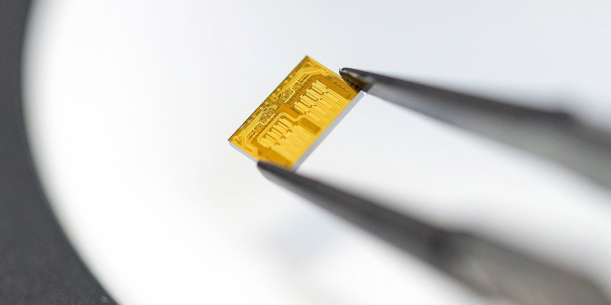
Nvidia has unveiled a prototype chip packaging technology that moves optical communication circuitry directly onto the silicon carrying its processors, a design the company says is meant to address data center power and bandwidth demands in future AI systems.
The company showed the technology, called Optics-on-Interposer (OOI), at SEMICON West 2026 in San Francisco, according to a report from Digitimes.
What the new design changes
Nvidia has unveiled a prototype of its next-generation co-packaged optics (CPO) technology, Optics-on-Interposer (OOI), at SEMICON West 2026. The design moves the optical engine from a conventional organic package substrate to the silicon interposer carrying the compute chips, increasing bandwidth density and reducing power consumption for future AI system interconnects.
In current AI servers, electrical signals traveling between processors and networking components lose energy as heat, and that loss grows worse as data centers pack in more chips to train and run AI models.
By fusing optical signaling directly into the interposer, the small piece of silicon that sits beneath and connects multiple chips in a package, Nvidia is betting it can keep pace with surging bandwidth needs without a matching surge in electricity use. The technology, called optics-on-interposer (OOI), moves optical engines from the organic package substrate onto the interposer that carries computing chips. Electrical signals travel directly through the interposer’s short, fine-pitch interconnects, similar to the architecture connecting graphics processing units (GPUs) and high-bandwidth memory (HBM).
Why the timing matters
The prototype reflects a broader scramble inside the chip industry to solve a power bottleneck as AI infrastructure scales.
Nvidia has already been rolling out its current generation of co-packaged optics products, and the company’s own newsroom has separately detailed related efforts to help data centers manage power constraints, including how companies are using NVIDIA DSX to address power limits, published around the same time as the interposer prototype announcement.
That power pressure has become a central theme across the AI hardware industry this year, as companies building ever larger GPU fleets look for ways to squeeze more performance out of every watt.
Nvidia’s own monitoring tools for sprawling GPU fleets, such as the system launched to track AI factory hardware, point to how much operational complexity has piled up around keeping these chips running efficiently at scale.
A long runway before deployment
Both OOI and a related dense wavelength-division multiplexing (DWDM) technology remain in the research stage, with no commercialization timeline announced, and Nvidia said it is evaluating them for potential future products.
The Digitimes report frames Nvidia’s work as groundwork for interconnect needs beyond 2028, giving its engineering teams and supply chain partners time to refine the manufacturing process before any commercial debut. Separate industry reporting on Nvidia’s broader co-packaged optics roadmap has pointed to scale-out revenue starting in H2 2026, scale-up volumes following in 2027, and customer deployments expected in 2028 as the window when such technology could appear in scale-up interconnects.
That long lead time is typical for packaging breakthroughs in the chip industry, where new interconnect schemes often take multiple product generations to move from prototype to mass production.
Nikola Nedovic, a principal researcher at Nvidia, presented the research at SEMICON West 2026 in San Francisco on Oct. 13.
Part of a wider chip arms race
The announcement lands amid intensifying competition in custom AI silicon, with rivals such as Tenstorrent raising fresh capital to challenge Nvidia’s hold on AI chips.
Cloud providers including Google have also pushed their own custom accelerators, while Nvidia continues to expand its lineup across data center GPUs, networking gear and now experimental packaging technology aimed at the back half of the decade.
Nvidia did not provide a specific production timeline or named customer for the Optics-on-Interposer design in its SEMICON West presentation, according to the Digitimes report.
The company is expected to share further technical details on co-packaged optics roadmaps at future GTC events as the technology moves closer to manufacturing readiness.
