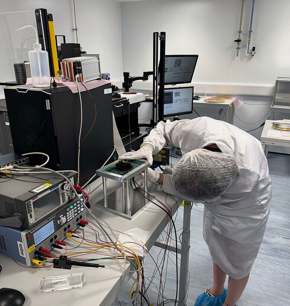
Inside a clean room lit like an operating theater, a technician lifts a square of coated glass no bigger than a dinner plate from a sealed plastic pod.
It looks like nothing, a mirror with faint lines etched across it.
That plate is one piece of a set a chipmaker will burn through for years.
Nobody outside the industry ever sees it, yet it sits behind every phone and AI server sold today.
So what does one of these sets actually cost, and why does that number matter right now?
Why one glass plate carries a price tag like a small company
A photomask, also called a reticle, is the master template that lets a beam of ultraviolet or extreme ultraviolet light stamp a circuit pattern onto silicon. In semiconductor manufacturing, photomasks are the master templates from which every chip is produced, and each reticle contains the circuit pattern for one layer of one product, an advanced processor can require dozens stacked in sequence.
At the newest nodes, that stacking adds up fast. A complete reticle set for a new product at 3nm node costs $20-30 million, requiring 60-100 individual reticles. The reason comes down to tolerance, since even a defect a few atoms wide can print onto every wafer exposed through that mask.
Extreme ultraviolet masks push that further. A single EUV reticle costs $300,000-500,000. Its thin protective membrane also wears out fast: when a pellicle includes no barrier layer and an anti-reflection layer made of Mo and a heat emissive layer made of Ru, the life of the pellicle is about 20,000 wafers before it must be replaced, according to a published patent filing.
A line item few people outside a fab ever see
Picture a chip design team finishing months of layout work, confident the hard part is behind them. Then the mask order lands on a budget sheet, and it rivals the cost of the engineering team itself.
That bill gets paid once per design, then spread across every wafer the mask ever prints, so volume producers absorb it more easily than smaller players. A company shipping tens of millions of units barely notices the mask line in its accounting.
A startup taping out a custom AI accelerator feels it immediately. That is part of why challengers like Tenstorrent have leaned on outside capital to keep scaling chip designs against Nvidia, the AI computing company closed $1.5B in Series E funding at a $6.2B post-money valuation, since the upfront tooling bill arrives long before any chip earns a dollar.
So the mask set functions as a quiet gatekeeper, rewarding scale over ambition.
Where the hardest numbers on this cost actually come from
Industry veterans who track photomask economics describe the pattern plainly. Mask pricing data gathered by suppliers and ERP vendors who track reticle costs shows the same climb: DUV reticles for mature nodes cost $10,000-50,000 each , a fraction of what the newest EUV sets demand.
That history matters, because extreme ultraviolet masks are following a similar curve to older nodes, just from a much higher base. The worldwide photomask production market was $3.1 billion in 2013 , and industry trackers expect that figure to keep climbing as EUV adoption spreads, though precise forecasts for the rest of this decade vary by source.
The physical cause keeps compounding too. Industry engineers have described needing duplicate masks to keep scanners running while originals are inspected or cleaned, since pellicles are not always viable at high throughput.
Patent filings add a concrete figure here: one pellicle design with no barrier layer and an anti-reflection layer made of Mo and a heat emissive layer made of Ru is rated for about 20,000 wafers , while improved versions with an alloy heat emissive layer can stretch that up to about 50,000 wafers, and designs that add a barrier layer can reach up to about 80,000 wafers .
Where this cost does not tell the whole story
None of this means every chip on a shelf today cost tens of millions just in tooling. Older nodes used in cars, appliances and simple electronics still rely on masks costing tens of thousands of dollars, a fraction of the leading edge bill.
So the dramatic figure applies narrowly, to the newest processors chasing the smallest transistors. Mask spending is not the only cost squeezing designers right now, either.
Advanced packaging, the step bonding a finished chip to memory, has become its own bottleneck. Suppliers are reportedly weighing price hikes of up to 20 percent as demand outruns capacity.
Mask costs have historically fallen once a node matures. Whether extreme ultraviolet masks follow that same decline is still an open question.
What it means for the next wave of chip startups
For an ordinary reader, the mask set is a reminder that a phone chip or an AI processor is not just clever engineering, it is a massive fixed bet placed before a single unit ships. That bet increasingly favors scale.
Even software companies feel the downstream pressure. The same AI boom straining mask shops and packaging lines is also reshaping pricing on tools like the coding assistants that run on the chips these masks print.
Which is why firms able to spread a $30 million tooling bill across tens of millions of chips keep pulling further ahead. That gap is not permanent, since cheaper EUV tooling has narrowed similar cost curves before.
For now, that plate of etched glass remains one of the most expensive, least visible objects in modern manufacturing, a quiet gatekeeper deciding which chip ideas ever reach a wafer at all.
